
Supervisor: Dr. Joe Smerdon
Scanning tunneling microscopy and low energy electron diffraction will be used to investigate graphene grown epitaxially on surfaces with large unit cells. The purpose of this investigation is to discover how to influence the graphene during growth so that it forms with a patterned character.
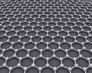
Graphene, the wonder material that won Andre Geim the Nobel Prize in 2010, looks set to revolutionise the world of technology. It is flexible, thin, transparent and more conductive than copper. In addition, it can be made in several shapes, for example hexagonal plates, continuous films and even zig-zag ribbons. Each of these shapes has a different electronic character. However, the palette of shapes is currently limited; if any shape desired could be patterned, whole circuits could be drawn out. Even electronic components such as transistors could be made just by drawing a particular shape in the graphene at a particular location in the circuit.
The most technologically relevant and scaleable method of manufacturing graphene is currently via growth on a metallic substrate, from which it can then be lifted and used as a component. The PhD project involves using new kinds of substrates to influence the growth of the graphene so that it can be patterned during growth. This patterning will result in changes to the electronic structure of the graphene, optimising its properties for use in various technologies, for example solar cells or display panels.
Atomic-scale microscopy, diffraction and compositional analysis will be undertaken, using facilities available within the new Nanophysics laboratory recently established at UCLan. Where appropriate, additional experiments will be conducted using the advanced facilities available within other laboratories in the UK such as Diamond Light Source in Oxfordshire and the Surface Science Research Centre in Liverpool.